Graphene possesses many outstanding properties: it conducts heat and electricity, it is transparent, harder than diamond and extremely strong.
But in order to use it to construct electronic switches, a material must not only be an outstanding conductor, it should also be switchable between ”on” and ”off” states. This requires the presence of a so-called bandgap, which enables semiconductors to be in an insulating state.
The problem, however, is that the bandgap in graphene is extremely small. Empa researchers from the ”nanotech@surfaces” laboratory thus developed a method some time ago to synthesise a form of graphene with larger bandgaps by allowing ultra-narrow graphene nanoribbons to ”grow” via molecular self-assembly.
In-Depth Article
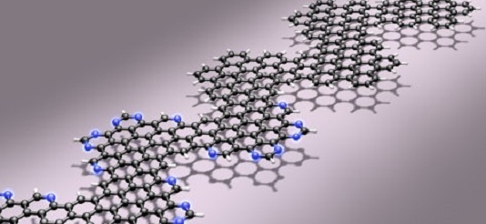
Graphene nanoribbons made of differently doped segments
The researchers, led by Roman Fasel, have now achieved a new milestone by allowing graphene nanoribbons consisting of differently doped subsegments to grow. Instead of always using the same ”pure” carbon molecules, they used additionally doped molecules – molecules provided with ”foreign atoms” in precisely defined positions, in this case nitrogen.
By stringing together ”normal” segments with nitrogen-doped segments on a gold (Au (111)) surface, so-called heterojunctions are created between the individual segments. The researchers have shown that these display similar properties to those of a classic p-n-junction, i.e. a junction featuring both positive and negative charges across different regions of the semiconductor crystal, thereby creating the basic structure allowing the development of many components used in the semiconductor industry.
A p-n junction causes current to flow in only one direction. Because of the sharp transition at the heterojunction interface, the new structure also allows electron/hole pairs to be efficiently separated when an external voltage is applied, as demonstrated theoretically by theorists at Empa and collaborators at Rensselaer Polytechnic Institute The latter has a direct impact on the power yield of solar cells. The researchers describe the corresponding heterojunctions in segmented graphene nanoribbons in the recently published issue of “Nature Nanotechnology”.
Transferring graphene nanoribbons onto other substrates
In addition, the scientists have solved another key issue for the integration of graphene nanotechnology into conventional semiconductor industry: how to transfer the ultra-narrow graphene ribbons onto another surface? As long as the graphene nanoribbons remain on a metal substrate (such as gold used here) they cannot be used as electronic switches. Gold conducts and thus creates a short-circuit that “sabotages” the appealing semiconducting properties of the graphene ribbon.
Fasel’s team and colleagues at the Max-Planck-Institute for Polymer Research in Mainz have succeeded in showing that graphene nanoribbons can be transferred efficiently and intact using a relatively simple etching and cleaning process onto (virtually) any substrate, for example onto sapphire, calcium fluoride or silicon oxide.
Graphene is thus increasingly emerging as an interesting semiconductor material and a welcome addition to the omnipresent silicon. The semiconducting graphene nanoribbons are particularly attractive as they allow smaller and thus more energy efficient and faster electronic components than silicon.
However, the generalized use of graphene nanoribbons in the electronics sector is not anticipated in the near future, due in part to scaling issues and in part to the difficulty of replacing well-established conventional silicon-based electronics. Fasel estimates that it may still take about 10 to 15 years before the first electronic switch made of graphene nanoribbons can be used in a product.
Graphene nanoribbons for photovoltaic components
Photovoltaic components could also one day be based on graphene. In a second paper published in «Nature Communications», Pascal Ruffieux – also from the Empa “nanotech@surfaces” laboratory – and his colleagues describe a possible use of graphene strips, for instance in solar cells.
Ruffieux and his team have noticed that particularly narrow graphene nanoribbons absorb visible light exceptionally well and are therefore highly suitable for use as the absorber layer in organic solar cells. Compared to “normal” graphene, which absorbs light equally at all wavelengths, the light absorption in graphene nanoribbons can be increased enormously in a controlled way, whereby researchers “set” the width of the graphene nanoribbons with atomic precision.
Publication References:
– Richard Denk et al: Exciton-dominated optical response of ultra-narrow graphene nanoribbons. Nature Communications, 2014.
– Jinming Cai et al: Graphene nanoribbon heterojunctions. Nature Nanotechnology, 2014.








Comments