One of the fastest-growing areas of solar energy research is with materials called perovskites. These promising light harvesters could revolutionize the solar and electronics industries because they show potential to convert sunlight into electricity more efficiently and less expensively than today’s silicon-based semiconductors.
These superefficient crystal structures have taken the scientific community by storm in the past few years because they can be processed very inexpensively and can be used in applications ranging from solar cells to light-emitting diodes (LEDs) found in phones and computer monitors.
A new study published online April 30 in the journal Science by University of Washington and University of Oxford researchers demonstrates that perovskite materials, generally believed to be uniform in composition, actually contain flaws that can be engineered to improve solar devices even further.
“Perovskites are the fastest-growing class of photovoltaic material over the past four years,” said lead author Dane deQuilettes, a UW doctoral student working with David Ginger, professor of chemistry and associate director of the UW Clean Energy Institute.
“In that short amount of time, the ability of these materials to convert sunlight directly into electricity is approaching that of today’s silicon-based solar cells, rivaling technology that took 50 years to develop,” deQuilettes said. “But we also suspect there is room for improvement.”
The research team used high-powered imaging techniques to find defects in the perovskite films that limit the movement of charges and, therefore, limit the efficiency of the devices. Perovskite solar cells have so far have achieved efficiencies of roughly 20 percent, compared to about 25 percent for silicon-based solar cells.
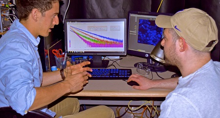
In a collaboration made possible by the Clean Energy Institute, the team used a technique called confocal optical microscopy, which is more often used in biology, and applied it to semiconductor technology. They used fluorescent images and correlated them with electron microscopy images to find “dark” or poorly performing regions of the perovskite material at intersections of the crystals. In addition, they discovered that they could “turn on” some of the dark areas by using a simple chemical treatment.
The images offered several surprises but also will lead to accelerated improvements in the materials’ uniformity, stability and efficiency, according to corresponding author Ginger, the Alvin L. and Verla R. Kwiram Endowed Professor of Chemistry and Washington Research Foundation Distinguished Scholar.
“Surprisingly, this result shows that even what are being called good, or highly-efficient perovskite films today still are ‘bad’ compared to what they could be. This provides a clear target for future researchers seeking to improve and grow the materials,” Ginger said.
The imaging technique developed by the UW team also offers an easy way to identify previously undiscovered flaws in perovskite materials and to pinpoint areas where their composition can be chemically altered to boost performance, Ginger said.
deQuilettes, who spearheaded the project as a Clean Energy Institute graduate fellow, estimates there are more than a thousand laboratories around the world currently researching the semiconducting properties of perovskite materials. Yet there is more work to be done to understand how to consistently make a material that is stable, has uniform brightness and can stand up to moisture without degrading. The UW research offers new ways for people to think strategically about how to improve the materials and how to extend their applications to high performance light-emitting devices such as LEDs and lasers.
“There are so many of us focusing on perovskites, so hopefully this technique will offer some new direction and steer us toward the places we can look to optimize their energy-capturing and emitting potential,” deQuilettes said.
Reference(s):
Publication: Dane W. Dequilettes, Sarah M. Vorpahl, Samuel D. Stranks, Hirokazu Nagaoka, Giles E. Eperon, Mark E. Ziffer, Henry J. Snaith, David S. Ginger. Impact of microstructure on local carrier lifetime in perovskite solar cells. Science, 2015
Story: Engineering a better solar cell: UW research pinpoints defects in popular perovskites | University of Washington — April 30, 2015






Comments