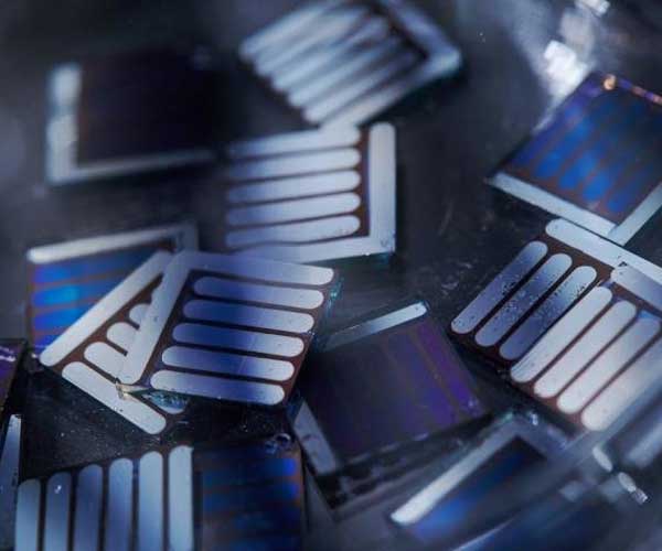
Organic solar cells (OSCs) has driven their efficiencies to above 10% to reach a viable level for commercialization. However, the increase in the photoactive layer thickness has resulted in lower efficiency levels, which therefore brings much complex manufacturing process.
A research team, led by Professor Changduk Yang and his research team in the School of Energy and Chemical Engineering at UNIST, has introduced a novel method that can solve issues associated with the thickness of the photoactive layers in OSCs.
In the study, the research team has succeeded in obtaining an efficiency of 12.01% in the organic solar cells, using a non-fullerance acceptor (IDIC) in the photoactive layer. Moreover, the new photoactive layer maintained its initial efficiency, even when the maximum measured thickness being in the range of 300 nm. This will help accelerate the design process, as well as the further commercialization of OSCs.
“Photoactive layers in the existing OSCs are rather thin (100 nm), and therefore it has been impossible to handle them via a large-area printing process,” says Professor Yang. “The new photoactive layer maintained its initial efficiency, even when the maximum measured thickness being in the range of 300 nm.”
Conventional solar cells are inorganic solar cells that are made of silicon (Si) semiconductors. While these solar cells are highly efficient and stable, they are inflexible and expensive, thus challenging to produce. Therefore, in recent years, lightweight organic solar cells (OSCs) and perovskite solar cells have gained much attention as the promising candidates for next-generation solar cells.
Although OSCs do exhibit high stability and reproducibility, the efficiency level of OSCs is not nearly as high as that of the perovskite solar cells. In the study, Professor Yang has solved the issues associated with the thickness of the photoactive layers in OSCs, thereby taking a step closer to the realization of a large-area printing process.
Photoactive layers used in solar cells convert solar energy into electrical energy. When these layers are exposed to sunlight, the excited electrons escape from the atom and generate free electrons and holes in a semiconductor. Here, the electrical energy is supplied by the movement of electrons and holes. The transfer of electrons is referred to as ‘Channel I’, while the movement of holes refers to as ‘Channel II’.
“Fullerene-based solar cells utilize only ‘Channel I due to inefficient light absorption in the thin active layers,” says Sang Myeon Lee in the Combined M.S./Ph.D. program in the School of Energy and Chemical Engineering at UNIST, the first author of the study. “New solar cells are capable of utilizing both Channel I and Channel II, thereby realizing high-efficiency level of 12.01%.”
“This study highlights the importance of optimizing the trade-off between charge separation/transport and domain size to achieve high-performance NF-PSCs,” says Professor Yang. “We will contribute to the production and commercialization of high efficiency organic solar cells in the future.”
“Our study presents a new pathway for the synthesis of non-fullerene photoactive materials,” says Professor Yang. “We hope to further contribute to the production and commercialization of high-efficient OSCs cell.”
Journal Reference:
Shanshan Chen, Sang Myeon Lee, Jianqiu Xu, Jungho Lee, Kyu Cheol Lee, Tianyu Hou, Yankang Yang, Mingyu Jeong, Byongkyu Lee, Yongjoon Cho, Sungwoo Jung, Jiyeon Oh, Zhi-Guo Zhang, Chunfeng Zhang, Min Xiao, Yongfang Li, Changduk Yang. Ultrafast Channel II process induced by a 3-D texture with enhanced acceptor order ranges for high-performance non-fullerene polymer solar cells. Energy & Environmental Science, 2018; DOI: 10.1039/C8EE01546E


Comments