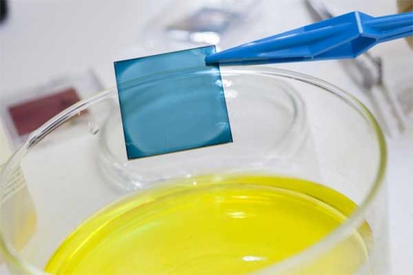
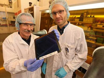
With a new technique for manufacturing single-layer organic polymer solar cells, scientists at UC Santa Barbara and three other universities might very well move organic photovoltaics into a whole new generation of wearable devices and enable small-scale distributed power generation.
The simple doping solution-based process involves briefly immersing organic semiconductor films in a solution at room temperature. This technique, which could replace a more complex approach that requires vacuum processing, has the potential to affect many device platforms, including organic printed electronics, sensors, photodetectors and light-emitting diodes. The researchers’ findings appear in the journal Nature Materials.
“Because the new process is simple to use, general in terms of applicability and should be configurable into mass productions, it has the potential to greatly accelerate the widespread implementation of plastic electronics, of which solar cells are one example,” said co-author Guillermo Bazan, director of UCSB’s Center for Polymers and Organic Solids. “One can see impacts in technologies ranging from light-emitting devices to transistors to transparent solar cells that can be incorporated into building design or greenhouses.”
Studied in many academic and industrial laboratories for two decades, organic solar cells have experienced a continuous and steady improvement in their power conversion efficiency with laboratory values reaching 13 percent compared to around 20 percent for commercial silicon-based cells. Though polymer-based cells are currently less efficient, they require less energy to produce than silicon cells and can be more easily recycled at the end of their lifetimes.
This new method, which provides a way of inducing p-type electrical doping in organic semiconductor films, offers a simpler alternative to the air-sensitive molybdenum oxide layers used in the most efficient polymer solar cells. Thin films of organic semiconductors and their blends are immersed in polyoxometalate solutions in nitromethane for a brief time — on the order of minutes. The geometry of these new devices is unique as the functions of hole and electron collection are built into the light-absorbing active layer, resulting in the simplest single-layer geometry with few interfaces.
“High-performing organic solar cells require a multiple layer device structure,” said co-author Thuc-Quyen Nguyen, a professor in UCSB’s Department of Chemistry and Biochemistry. “The realization of single-layer photovoltaics with our approach will simplify the device fabrication process and therefore should reduce the cost. The initial lifetime testing of these single layer devices is promising. This exciting development will help transform organic photovoltaics into a commercial technology.”
Organic solar cells are unique within the context of providing transparent, flexible and easy-to-fabricate energy-producing devices. These could result in a host of novel applications, such as energy-harvesting windows and films that enable zero-cost farming by creating greenhouses that support crops and produce energy at the same time.
Reference(s):
Publication: Vladimir A. Kolesov, Canek Fuentes-Hernandez, Wen-Fang Chou, Naoya Aizawa, Felipe A. Larrain, Ming Wang, Alberto Perrotta, Sangmoo Choi, Samuel Graham, Guillermo C. Bazan, Thuc-Quyen Nguyen, Seth R. Marder, Bernard Kippelen. Solution-based electrical doping of semiconducting polymer films over a limited depth. Nature Materials, 2016
Research story: University of California – Santa Barbara | December 06, 2016 (source)


Comments