


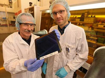
- Versatile compounds called perovskites are valued for their application in next-generation solar energy technologies.
- Despite their efficiency and relative cheapness, perovskite devices have yet to be perfected; they often contain atomic-level structural defects.
- Scientists have, for the first time, characterized the structural defects that prompts the movement of ions, destabilizing the perovskite materials.
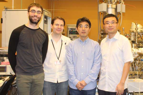
Professor Yabing Qi and his team in the Energy Materials and Surface Sciences Unit at OIST, in collaboration with researchers at the University of Pittsburgh, USA, have, for the first time, characterized the structural defects that prompt the movement of ions, destabilizing the perovskite materials. The researchers’ findings, published in ACS Nano, may inform future engineering approaches to optimize perovskite solar cells.
“For a long time, scientists have known structural defects exist, but didn’t understand their precise chemical nature,” said Collin Stecker, an OIST Ph.D. student and the first author of the study. “Our study delves into fundamental characteristics of perovskite materials to help device engineers further improve them.”
Surface-level issues
Perovskite compounds share a unique structure that makes them useful in electronics, engineering, and photovoltaics. They are exceptional at absorbing light, as well as generating and transporting charge carriers responsible for current in semiconductor materials. Sandwiching perovskite materials between other functional layers forms perovskite solar cells. However, defects in the perovskite layer can disrupt charge transfer between the perovskite and adjacent layers of the cell, hindering the device’s overall performance and stability.
To understand the electronic and dynamic properties of these perovskite defects, the OIST researchers used a method called scanning tunneling microscopy to take high-resolution images of the movements of individual ions on the perovskite surfaces.
Upon analyzing these images, Stecker and his colleagues noticed groups of vacant spaces across the surfaces where atoms were missing. In addition, they saw that pairs of Br- (bromide) ions on the perovskite surfaces were shifting and changing direction. The researchers’ collaborators at the University of Pittsburgh performed a series of theoretical calculations to model the pathways these ions took, supporting these experimental observations.
The OIST scientists concluded that the surface vacancies were likely causing these ions to move across the perovskite materials. Understanding this mechanism of ion movement may later help scientists and engineers mitigate the structural and functional consequences of these defects.
The researchers acknowledged that, although perovskites are promising alternatives to the widely used silicon, the technology needs to be refined before it’s commercialized.
“These perovskite surfaces are much more dynamic than we previously anticipated,” said Stecker. “Now, with these new findings, we hope engineers can better account for the effect of defects and their motion in order to improve devices.”


Comments