Researchers at the Department of Energy’s Oak Ridge National Laboratory have found a potential path to further improve solar cell efficiency by understanding the competition among halogen atoms during the synthesis of sunlight-absorbing crystals.
Photovoltaic cells that convert sunlight directly into electricity are becoming increasingly prominent in the world’s renewable energy mix. One promising area of solar energy research involves perovskites, a material that can potentially convert sunlight into electricity more efficiently and less expensively than typical silicon-based semiconductors.
Perovskite-based solar cells, however, have been hindered by unreliable durability, poor efficiency and unresolved questions.
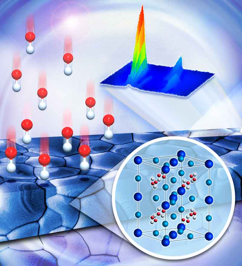
 Oak Ridge National Laboratory scientists combined imaging techniques to measure crystallization kinetics of perovskite films following exposure to a mixed halide vapor. Over time, extra halide reactants settle in the film’s grain boundaries, demonstrating atomic competition in crystal growth. Image by ORNL’s Jill Hemman.
“Organometallic halide perovskite semiconductors have high carrying capacity and efficiency to rival silicon-based solar cells. These materials are easy and cheap to grow but have been known to degrade,” said Bin Yang, an ORNL postdoctoral researcher at the Center for Nanophase Materials Science.
A new study published in the Journal of the American Chemical Society demonstrates that in the presence of reactive iodide ions, negatively charged bromine and chlorine are left out of the final perovskite crystal structure – like not making the team in gym class.
“To take that first step and maximize solar cell technology made with organometallic halide perovskites, we need to know how to grow high quality light-absorbing material and establish optimal film growth processes,” said Yang, the study’s lead author. “The simple printing or spraying of perovskite ink makes solar module costs even lower.”
Using high-powered imaging techniques, Yang and the team tracked kinetic activity in organometallic halide perovskites.
Halogen ions, jockeying for a position in the growing structure, affect the movement of charges through the crystals and subsequently impact the efficiency of sunlight’s conversion to electricity.
“The kinetic activity found in halide perovskites poses significant challenges for advancing high-efficiency optoelectronic materials and devices,” said Kai Xiao, study co-author and ORNL staff scientist.
The team first used X-ray diffraction for a real-time peek at the stages of crystallization, immediately monitoring the chemical reaction between a mixed-halide vapor and a thin lead-iodide film.
ORNL researchers then extracted chemical, molecular and elemental data from the perovskites using time-of-flight secondary ion mass spectrometry for ex-situ analysis. The mass spectrometer’s beams of ions provided a snapshot of information about molecular activity on the crystal’s surface and established chlorine’s eventual distribution in the grain boundaries, or crevices, of perovskite films.
A combination of imaging techniques allowed the ORNL team to track the outcome of the halogen competition in the solar material.
Researchers discovered that while bromine, chlorine and iodine ions facilitate growth in a developing organometallic perovskite structure, only iodine gets a spot in the final crystal. However, though they are left out of the final structure, the molecules build “team morale” as they help promote overall crystal growth.
The measurements offered several insights into perovskite crystallization kinetics that will lead to improvements in the synthesis and processing of the materials for high efficiency solar cells, according to Xiao.
“Identifying the chemical phenomenon of halide competition in hybrid perovskites will help in engineering large-grain perovskite films for better, cheaper solar devices,” Xiao said.
Co-authors of the study are ORNL’s Jong Keum, Olga Ovchinnikova, Alex Belianinov, Mao-Hua Du, Ilia Ivanov, Christopher Rouleau, and David Geohegan, and East China Normal University’s Shiyou Chen.
This research was conducted at the Center for Nanophase Materials Sciences (CNMS), which is a DOE Office of Science User Facility. The work was supported by DOE’s Office of Science.
Story: DOE/Oak Ridge National Laboratory


Comments