


Laser processing produces deep ripples in silicon over a wide area — something that could enhance solar cell efficiency.
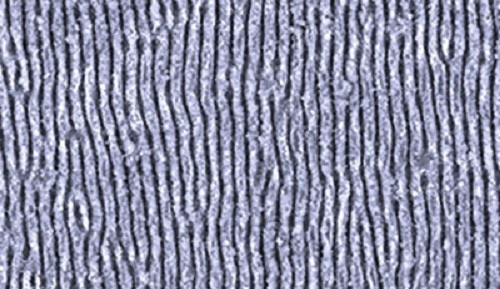
A*STAR scientists have produced a uniform nanoscale ripple pattern over a wide area on a silicon surface by scanning a femtosecond laser beam across it. Given that a rippled surface is much less reflective than a smooth surface, this simple innovation could enhance the efficiency of solar cells by boosting their ability to harvest more sunlight1.
The use of lasers to produce periodic surface structures is currently an area of intense research. Laser processing has the important advantage that it heats only the surface of a material, leaving underlying structures unaffected. However, many laser processing methods are limited: they can process only small areas and shallow ripples.
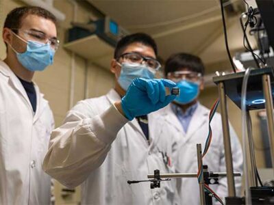
Now, Xincai Wang and co-workers from A*STAR’s Singapore Institute of Manufacturing Technology and Nanyang Technological University have successfully addressed these limitations. They demonstrate the potential of their technique by using it to produce a uniform ripple pattern on a silicon substrate (see image) over a large area of 30 millimeters by 30 millimeters, with an average ripple depth of 300 nanometers — about three times greater than that of other techniques.
“This increase in depth can substantially reduce light reflection and improve the light-trapping ability of the ripple structure,” Wang notes. “Hence, if the structure is used in photovoltaic devices, more light will be trapped within the structure, thereby enhancing the device efficiency.”
Straightforward and inexpensive, the technique simply involves using a cylindrical lens to widen a femtosecond laser beam to a width of 50 micrometers and then scanning the beam across the surface.
As the energy of the laser’s photons exceeds the bandgap of silicon, the photons excite electrons from the valence band to the conduction band. Such electrons would usually relax by transferring their energy to the atomic lattice, thereby heating it. However, the extremely short pulse durations mean that instead they generate an electron wave on the surface. This in turn produces a light wave, which interferes with the incoming laser beam. The silicon is removed in locations where the incoming and outgoing light waves constructively interfere with each other, giving rise to the valleys in the ripple pattern.
The researchers found that on rippling the average reflectance of a silicon surface dropped from 39.7 per cent to 12.5 per cent, which meant light absorption was enhanced by 41 per cent as a result of strong scattering by the ripple structure. This effect could be exploited to manage photon behavior in solar cells and light-emitting diodes.
References:
Publication: L. Hong, Rusli, X.C. Wang, H.Y. Zheng, H. Wang, H.Y. Yu. Femtosecond laser fabrication of large-area periodic surface ripple structure on Si substrate. Applied Surface Science, 2014
Story Source: Making waves with lasers. The Agency for Science, Technology and Research (A*STAR) — January 20, 2015


Comments