


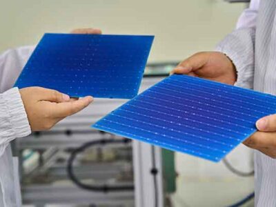
A team of researchers led by North Carolina State University has found that stacking materials that are only one atom thick can create semiconductor junctions that transfer charge efficiently, regardless of whether the crystalline structure of the materials is mismatched – lowering the manufacturing cost for a wide variety of semiconductor devices such as solar cells, lasers and LEDs.
“This work demonstrates that by stacking multiple two-dimensional (2-D) materials in random ways we can create semiconductor junctions that are as functional as those with perfect alignment” says Dr. Linyou Cao, senior author of a paper on the work and an assistant professor of materials science and engineering at NC State.
“This could make the manufacture of semiconductor devices an order of magnitude less expensive.”
For most semiconductor electronic or photonic devices to work, they need to have a junction, which is where two semiconductor materials are bound together. For example, in photonic devices like solar cells, lasers and LEDs, the junction is where photons are converted into electrons, or vice versa.
All semiconductor junctions rely on efficient charge transfer between materials, to ensure that current flows smoothly and that a minimum of energy is lost during the transfer. To do that in conventional semiconductor junctions, the crystalline structures of both materials need to match. However, that limits the materials that can be used, because you need to make sure the crystalline structures are compatible. And that limited number of material matches restricts the complexity and range of possible functions for semiconductor junctions.
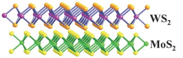
“But we found that the crystalline structure doesn’t matter if you use atomically thin, 2-D materials,” Cao says. “We used molybdenum sulfide and tungsten sulfide for this experiment, but this is a fundamental discovery that we think applies to any 2-D semiconductor material. That means you can use any combination of two or more semiconductor materials, and you can stack them randomly but still get efficient charge transfer between the materials.”
Currently, creating semiconductor junctions means perfectly matching crystalline structures between materials – which requires expensive equipment, sophisticated processing methods and user expertise. This manufacturing cost is a major reason why semiconductor devices such as solar cells, lasers and LEDs remain very expensive. But stacking 2-D materials doesn’t require the crystalline structures to match.
“It’s as simple as stacking pieces of paper on top of each other – it doesn’t even matter if the edges of the paper line up,” Cao says.
Publication Reference:
Yifei Yu, Shi Hu, Liqin Su, Lujun Huang, Yi Liu, Zhenghe Jin, Alexander A Purezky, David B. Geohegan, Ki Wook Kim, Yong Zhang, Linyou Cao. Equally Efficient Interlayer Exciton Relaxation and Improved Absorption in Epitaxial and Non-epitaxial MoS2/WS2 Heterostructures. Nano Letters, 2014
Article Source:
Stacking Two-Dimensional Materials May Lower Cost of Semiconductor Devices; North Carolina State University — December 11, 2014


Comments