To understand the nature of something extremely complex, you often have to study its smallest parts. In trying to decipher the universe, for example, we search for gravitational waves or faint waves of light from the Big Bang.
And to comprehend the very essence of matter itself, we break it down to the subatomic level and use computer simulations to study particles like quarks and gluons.
Understanding materials with specific functions, such as those used in solar cells, and engineering ways to improve their properties pose many of the same challenges. In the ongoing effort to improve solar cell energy conversion efficiencies, researchers have begun digging deeper — in some cases to the atomic level — to identify material defects that can undermine the conversion process.
For example, heterogeneous nanostructured materials are widely used in a variety of optoelectronic devices, including solar cells. However, due to their heterogeneous nature, these materials contain nanoscale interfaces exhibiting structural defects that can affect the performance of these devices.

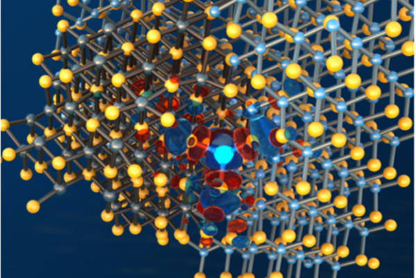
Cross section of the interface between a lead chalcogenide nanoparticle and its embedding cadmium chalcogenide matrix. When integrated into optoelectronic devices, it is enough to have a single atom in the wrong place at the interface (represented by the glowing blue color) to jeopardize their performance. (Illustration: Peter Allen, Institute for Molecular Engineering, University of Chicago)
It is very challenging to identify these defects in experiments, so a team of researchers at the Department of Energy’s Argonne National Laboratory and the University of Chicago decided to run a series of atomistic calculations at Lawrence Berkeley National Laboratory’s National Energy Research Scientific Computing Center (NERSC) to find the root cause of defects in two commonly used semiconductor materials — lead selenide (PbSe) and cadmium selenide (CdSe) — and provide design rules to avoid them.
“We are interested in understanding quantum dots and nanostructures and how they perform for solar cells,” said Giulia Galli, Liew Family professor of Molecular Engineering at the University of Chicago and co-author of a paper published in Nano Letters that outlines this work and its findings. “We are doing modeling, using both classical molecular dynamics and first principle methods, to understand the structure and optical properties of these nanoparticles and quantum dots.”
Core-shell Nanoparticles
For this study, the team focused on heterostructured nanoparticles — in this case a colloidal quantum dot in which PbSe nanoparticles are embedded in CdSe. This type of quantum dot — also known as a core-shell nanoparticle — is like an egg, Márton Vörös, Aneesur Rahman Fellow at Argonne and co-author on the paper, explained, with a “yolk” made of one material surrounded by a “shell” made of the other material.
“Experiments have suggested that these heterostructured nanoparticles are very favorable for solar energy conversion and thin-film transistors,” Vörös said.
For example, while colloidal quantum dot energy conversion efficiencies currently hover around 12% in the lab, “we aim at predicting quantum dot structural models to go beyond 12%,” said Federico Giberti, postdoctoral research scholar at the University of Chicago’s Institute for Molecular Engineering and first author on the Nano Letters paper. “If 20% efficiency could be reached, we would then have a material that becomes interesting for commercialization. ”
To make this happen, however, Vörös and Giberti realized they needed to better understand the structure of nanoscale interfaces and whether atomistic defects were present. So, along with Galli, they developed a computational strategy to investigate, at the atomic level, the effect of the structure of the interfaces on the materials’ optoelectronic properties. By using classical molecular dynamics and first principles methods that do not rely on any fitted parameters, their framework allowed them to build computational models of these embedded quantum dots.
Using this model as the basis for a series of simulations run at NERSC, the research team was able to characterize PbSe/CdSe quantum dots and found that atoms that are displaced at the interface and their corresponding electronic states — what they call “trap states” — can jeopardize solar cell performance, Giberti explained. They were then able to use the model to predict a new material that does not have these trap states and should perform better in solar cells.
“Using our computational framework, we also found a way to tune the optical properties of the material by applying pressure,” Giberti added.
This research — which included studies of electron and atomic structures — used four million supercomputing hours at NERSC, according to Vörös. Most of the atomic structure calculations were run on Cori, NERSC’s 30-petaflop system installed in 2016, although they also used the Edison system, a Cray XC30 with Intel Xeon processors. While the calculations didn’t need a large number of processors, Giberti noted, “I needed to launch many simultaneous simulations at the same time, and analyzing all the data was in itself a rather challenging task.”
Looking ahead, the research team plans to use this new computational framework to investigate other materials and structures.
“We believe that our atomistic models, when coupled with experiments, will bring a predictive tool for heterogeneous nanostructured materials that can be used for a variety of semiconducting systems,” Federico said. “We are very excited about the possible impact of our work.”
Reference(s):
1. Publication: Federico Giberti, Márton Vörös, Giulia Galli. Design of Heterogeneous Chalcogenide Nanostructures with Pressure-Tunable Gaps and without Electronic Trap States. Nano Letters, 2017
2. Research story: DOE/Lawrence Berkeley National Laboratory | June 9, 2017 (source)


Comments