Solar cell efficiency has soared in recent years due to light-harvesting materials like halide perovskites, but the ability to produce them reliably at scale continues to be a challenge.
A process developed by Rice University chemical and biomolecular engineer Aditya Mohite and collaborators at Northwestern University, the University of Pennsylvania and the University of Rennes yields 2D perovskite-based semiconductor layers of ideal thickness and purity by controlling the temperature and duration of the crystallization process.
Known as kinetically controlled space confinement, the process could help improve the stability and reduce the cost of halide perovskite-based emerging technologies like optoelectronics and photovoltaics.

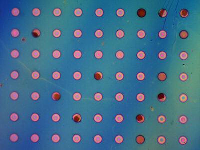
A process developed by Rice engineers and collaborators yields 2D halide perovskite crystal layers of ideal thickness and purity through dynamic control of the crystallization process–a key step toward ensuring device stability for optoelectronics and photovoltaics. (Jeff Fitlow/Rice University)
“Producing 2D perovskite crystals with layer thicknesses—or quantum well thickness, also known as ‘n value’—greater than two is a major bottleneck,” said Jin Hou, a Ph.D. student in Rice’s George R. Brown School of Engineering, who is a lead author on a study about the process published in Nature Synthesis. “An n value higher than four means materials have a narrower band gap and higher electrical conductivity—a crucial factor for application in electronic devices.”
As they form into crystals, atoms or molecules arrange themselves into highly organized, regular lattices. Ice, for instance, has 18 possible atomic arrangements, or phases. Like the hydrogen and oxygen atoms in ice, the particles that make up halide perovskites can also form multiple lattice arrangements. Because material properties are phase-dependent, scientists aim to synthesize 2D halide perovskite layers that exhibit only a single phase throughout.
The problem, however, is that traditional synthesis methods for higher n value 2D perovskites generate uneven crystal growth, which impacts the material’s performance reliability.
“In traditional methods of 2D perovskite synthesis, you get crystals with mixed phases due to the lack of control over crystallization kinetics, which is basically the dynamic interplay between temperature and time,” Hou said. “We designed a way to slow down the crystallization and tune each kinetics parameter gradually to hit the sweet spot for phase-pure synthesis.”
In addition to designing a synthesis method that can achieve a gradual n value increase in 2D halide perovskites, the researchers also created a map (phase diagram) of the process through characterization, optical spectroscopy and machine learning.
“This work pushes the boundaries of higher quantum well 2D perovskites synthesis, making them a viable and stable option for a variety of applications,” Hou said.
“We have developed a new method to improve the purity of the crystals and resolved a long-standing question in the field on how to approach high n value, phase-pure crystal synthesis,” said Mohite, an associate professor of chemical and biomolecular engineering and materials science and nanoengineering whose lab has pioneered various methods of improving halide perovskite semiconductor quality and performance, from calibrating the initial stage of crystallization to fine-tuning solvent design.
“This research breakthrough is critical for the synthesis of 2D perovskites, which hold the key to achieving commercially relevant stability for solar cells and for many other optoelectronic device applications and fundamental light matter interactions,” Mohite added.


Comments