


- Common semiconductor materials for solar cells, such as silicon, must be grown via an expensive process to avoid defects within their crystal structure that affect functionality.
- But metal-halide perovskite semiconductors are emerging as a cheaper, alternative material class, with excellent and tunable functionality as well as easy processability.
Climate change and its consequences are becoming increasingly obvious, and solar cells that convert the sun’s energy into electricity will play a key role in the world’s future energy supply.
Common semiconductor materials for solar cells, such as silicon, must be grown via an expensive process to avoid defects within their crystal structure that affect functionality. But metal-halide perovskite semiconductors are emerging as a cheaper, alternative material class, with excellent and tunable functionality as well as easy processability.
In APL Materials, from AIP Publishing, researchers present a road map for organic-inorganic hybrid perovskite semiconductors and devices.
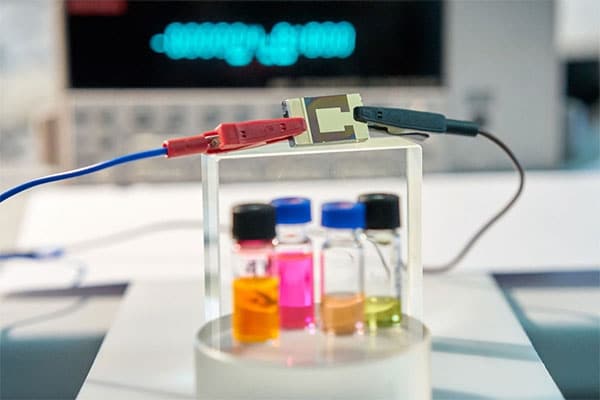
Perovskite semiconductors can be processed from solution, and a semiconductor ink can be coated or simply painted over surfaces to form the desired film. This can be incorporated into semiconductor devices, such as solar cells or light-emitting diodes.
“For many years, solution-processed semiconductors were viewed as unable to deliver the same functionality as specially grown crystalline semiconductors,” said Lukas Schmidt-Mende, a co-author from the University of Konstanz in Germany. “The reason behind this thinking was that simple solution processing will inherently lead to a relative high number of defects within the formed crystal structure, which can negatively affect its functionality.”
It turns out organic-inorganic hybrid perovskites are very defect-tolerant. Defects formed after processing do not dramatically influence device functionality, and for the first time, hybrid perovskites are enabling efficient solution-processed devices.
“We can simply change the chemical composition of the perovskite to tune its bandgap, which allows us to change the absorption profile,” said Schmidt-Mende. “This can be used to prepare light-emitting diodes at different wavelengths or to tune the perovskite material for tandem solar cells to optimize the absorption profile.”
High defect tolerance, however, “came as a surprise that needs to be better understood,” he said. “Understanding the details will help to further optimize the material, perhaps to find other similar efficient alternatives and give us the chance to improve applications based on perovskite semiconductors.”
The group points out that perovskite devices currently have two major drawbacks.
First, the most efficient devices all contain toxic lead and efforts to replace it with less toxic elements have so far been only partly successful. Second, perovskite devices have a reduced life span compared to silicon devices.
“Although the stability of perovskite devices has increased dramatically during the past few years, we still do not understand and have not overcome all of its degradation mechanisms,” said Schmidt-Mende.
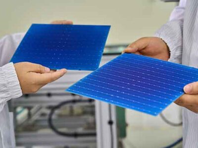
Many researchers are working on solar cells and, with the possibility of tuning the bandgap, perovskites are intriguing for tandem applications where they may be combined with an established silicon solar cell.
“Other applications are light-emitting diodes, where the color of the light emitted can be tuned by adjusting the chemical composition of the perovskite,” Schmidt-Mende said. “As for other semiconductors, the list of possible applications is long, and we are just beginning to understand this material and its potential.”
—
Publication Referenced in the Article:
Lukas Schmidt-Mende, Vladimir Dyakonov, Selina Olthof, Feray Ünlü, Khan Moritz Trong Lê, Sanjay Mathur, Andrei D. Karabanov, Doru C. Lupascu, Laura M. Herz, Alexander Hinderhofer, Frank Schreiber, Alexey Chernikov, David A. Egger, Oleksandra Shargaieva, Caterina Cocchi, Eva Unger, Michael Saliba, Mahdi Malekshahi Byranvand, Martin Kroll, Frederik Nehm, Karl Leo, Alex Redinger, Julian Höcker, Thomas Kirchartz, Jonathan Warby, Emilio Gutierrez-Partida, Dieter Neher, Martin Stolterfoht, Uli Würfel, Moritz Unmüssig, Jan Herterich, Clemens Baretzky, John Mohanraj, Mukundan Thelakkat, Clément Maheu, Wolfram Jaegermann, Thomas Mayer, Janek Rieger, Thomas Fauster, Daniel Niesner, Fengjiu Yang, Steve Albrecht, Thomas Riedl, Azhar Fakharuddin, Maria Vasilopoulou, Yana Vaynzof, Davide Moia, Joachim Maier, Marius Franckevičius, Vidmantas Gulbinas, Ross A. Kerner, Lianfeng Zhao, Barry P. Rand, Nadja Glück, Thomas Bein, Fabio Matteocci, Luigi Angelo Castriotta, Aldo Di Carlo, Matthias Scheffler, Claudia Draxl. Roadmap on organic–inorganic hybrid perovskite semiconductors and devices. APL Materials, 2021; 9 (10): 109202 DOI: 10.1063/5.0047616
—
This article was written by American Institute of Physics


Comments